Tampilkan postingan dengan label Power Supply. Tampilkan semua postingan

Jumat, 11 Januari 2013

Simple 6-Input Alarm

This simple alarm circuit was designed for use in a combined garage and rumpus room. It can be assembled on Veroboard and uses just one IC plus a handful of cheap components. The circuit is based on a straightforward 555 timer circuit (IC1). This is wired as a monostable and sets the siren period which is adjustable up to about three minutes using potentiometer VR1. In operation, IC1's pin 2 input monitors the detector circuit for negative-going signals. When a switch is closed, a brief negative-going pulse is applied to pin 2 via a 10µF capacitor and its corresponding series diode (D2-D7). This triggers IC1 which switches its pin 3 output high and switches off relay RLY1 (ie, RLY1 is normally on).


 As a result, the piezo siren sounds for the duration of the monostable period. In addition, relay RLY2 is turned on via diode D9 and latches on via D10. This means that the strobe light (which is wired to the normally open contact) will continue to flash until the alarm is switched off (via the keyswitch). At the end of the monostable period, RLY1 turns off and this turns off the piezo siren. The circuit can then be retriggered by any further trigger inputs from the switches. A variety of detectors with normally open contacts can be used for the switches, including reed switches, pressure mats, IR detectors and glass breakage detectors. All switches must be open before the alarm is switched on.

Rabu, 02 Januari 2013

Low-Power Voltage Doubler (Booster)

All miniature electronic devices operate off batteries. Some of them need higher than the standard battery voltages to operate efficiently. If the battery of that specific voltage is unavailable, we are forced to connect additional cells in series to step up the DC voltage. Thus, the true meaning of miniaturisation is lost. A simple way to overcome this problem is to employ a voltage doubler, if the device under consideration can operate at a small current.

Here we present a low-power voltage doubler circuit that can be readily used with devices that demand higher voltage than that of a standard battery but low operating current to work with. The circuit is quite simple as it uses only a few components. Yet, the output efficiency is 75 to 85 percent along its operating voltage range. The available battery voltage is almost doubled at the output of the circuit.

Here IC1 is wired as an astable multivibrator to generate rectangular pulses at around 10 kHz. This frequency and duty cycle of the pulses can be varied using preset VR1. The pulses are applied to switching transistors T1 and T2 for driving the output section, which is configured as a voltage-doubling circuit. The doubled voltage is available across capacitor C5. During each cycle of the pulse occurance, the high level drives T1 into its saturation, keeping transistor T2 cut off.


So transistor T1 charges capacitor C4 via the path formed by diodes D2 and D1 to a voltage level slightly lesser than the supply. But during the low period of the pulse, transistor T1 is cut off while transistor T2 is driven into saturation. Now, transistor T2 raises the charge on the negative pole of capacitor C4 by another step equal to the supply voltage. Therefore an equal amount of charging is built up on capacitor C5 via diode D3.

This doubling action increases the total voltage across capacitor C5 to almost double the input voltage. If the output of the pulse generator is maintained with a high enough amplitude and frequency, the output voltage and current remain constant and cater to the needs of the load. Even with the half-wave function, this circuit is almost free of ripple voltage. If the connected load doesn’t require a high current, the efficiency can be expected in the upper 90 percentranges.

Since the input voltage is doubled, the current drain from the input power supply is also doubled at the input but halved at the output. One point of caution is that if the multivibrator’s frequency is fairly high, the output may suffer with the interference imposed over the DC voltage. In this case, the frequency must be set favorably by trials and actual load connection procedure. This tiny circuit can be assembled on the general-purpose PCB. If all of the components are surface-mount type, the whole module can be genuinely miniaturized.

EFY Lab note.
During testing with input of 8V and 1.25mA load current the output voltage was found to be around 13V.

Ampere or Current Booster Circuit

Volt regulators such as the LM708, and LM317 series (and others) sometimes need to provide a little bit more current then they actually can handle. If that is the case, this little circuit can help out. A power transistor such as the 2N3772 or similar can be used.
The power transistor is used to boost the extra needed current above the maximum allowable current provided via the regulator.
Current up to 1500mA(1.5amp) will flow through the regulator, anything above that makes the regulator conduct and adding the extra needed current to the output load. It is no problem stacking power transistors for even more current. (see diagram). Both regulator and power transistor must be mounted on an adequate heatsink.

 
Parts:

R1 = 1R-2W
R2 = 10R-2W
C1 = 35v-470uF
C2 = 35v-470uF
Q1 = TIP2955
IC1 = 78xx Regulator

Selasa, 11 Desember 2012

Fuse Saver

This circuit will be particularly useful to those hobbyists who use a ‘breadboard’ to try out ideas and who also use a simple ‘home-made’ DC power supply consisting of a transformer, rectifier, smoothing capacitor and protective fuse, that is, one without over current protection! In this circuit, the detecting element is resistor R6. Under normal conditions, its voltage drop is not high enough to switch on transistor T1.

The value of R6 can be altered to give a different cut-off current, as determined by Ohm’s Law, if required. When a short circuit occurs in the load, the voltage rises rapidly and T1 starts to conduct. This draws in the relay, switching its contacts, which cuts off power to the external circuit, and instead powers the relay coil directly, latching it in this second state. The circuit remains in this state until the primary power supply is switched off.

Capacitors C1 and C2 hold enough charge (via D3, D4 and D6, which prevent the charge from being lost to the rest of the circuit, whichever state it is in) to keep T1 switched on and power the relay while it switches over, and R2 and R4 provide slow discharge paths. LEDs D1 (red) and D5 (green) indicate what state the circuit is in. Inductor L1 slows the inrush of current when the circuit is switched on, which would otherwise cut off the circuit immediately


D2 and D7 provide the usual back-emf protection across the coils. In use, the input of the circuit is connected to the main transformer-rectifier-capacitor-fuse power supply via K1, and the output is connected to the (experimental) load via K2. Note that the input voltage must be a floating supply if Vout– is grounded via the load, as Vin– and Vout– must not be connected together. Some consideration needs to be given to a number of components.

First, the choice of relay Re1. For the prototype, this was obtained from Maplin, part number YX97F. This is has a coil resistance of 320 ?, which with R1 forms the collector load for T1. Its allowed pull-in voltage range is nominally 9 V to 19 V, which limits the input power supply voltage to between around 10 V to 30 V (DC only). R1 could be replaced by a wire link for operation at input voltages below 10 V, or increased in value, as determined by either the application of Ohm’s Law once more or trial and error, for an input voltage above 30 V.

Coil L1 was obtained from Farnell, part number 581-240. Finally, the protective fuse for the input power supply should be a ‘slow-blow’ type; ‘fast’ fuses will rupture before the relay has time to switch. Also note that this device is meant to save fuses, not replace them. A mains transformer must always be fused if it is not designed to run safely, i.e., without presenting a fire hazard, even if its output has a continuous short-circuit fault.

1.5 - 35 Volt DC Regulated Power Supply

The easy way to power your projects


Here is the circuit diagram of regulated power supply. It is a small power supply that provides a regulated voltage, adjustable between 1.5 and 35 volts at 1 ampere. This circuit is ready to use, you just need to add a suitable transformer. This circuit is thermal overload protected because the current limiter and thermal overload protection are included in the IC.

Circuit diagram:
 1A 1.5 volt to 35 volt dc Regulated Power Supply Circuit Diagram
1A Regulated Power Supply Circuit Diagram


Transformer selection chart:
  Transformer Selection Chart for 1A 1.5 volt to 35 volt dc Regulated Power Supply Circuit Diagram
Transformer selection Guide-Table For Power Supply


Parts:

IC = LM317
P1 = 4.7K
R1 = 120R
C1 = 100nF - 63V
C2 = 1uF - 35V
C3 = 10uF - 35V
C4 = 2200uF - 35V
D1-D4 = 1N4007


Features:
  • Just add a suitable transformer (see table)
  • Great to power your projects and save money on batteries
  • Suitable as an adjustable power supply for experiments
  • Control DC motors, low voltage light bulbs, …


Specifications :
  • Preset any voltage between 1.5 and 35V
  • Very low ripple (80dB rejection)
  • Short-circuit, thermal and overload protection
  • Max input voltage : 28VAC or 40VDC
  • Max dissipation : 15W (with heatsink)
  • Dimensions : 52x52mm (2.1” x 2.1”)


Technical Specifications
  • Input Voltage = 40Vdc max Transformer
  • Output Voltage = 1.5V to 35Vdc
  • Output Current = 1.5 Amps max.
  • Power Dissipation = 15W max (cooled)


Note:
  • It has not to be cooled if used for small powers. 28 Volt AC max is allowed for the input voltage.

3-30V 3A Adjustable Regulated DC Power Supply

A power supply for all general circuits, Based on a stablized DC voltage of 30 volt

This power supply is meant as an auxiliary or as a permanent power supply for all common circuits based on a stabilized DC voltage between 3 and 30V provided that the consumption does not exceed 3A. Of course this power supply unit can also be used for other purposes. Be replacing the trimmer by a potentiometer, it may even be used as an adjustable power supply unit. A good quality heatsink must be used.

Picture of project:

3 TO 30 Volt 3 Ampere DC Power Supply
Circuit diagram:
 3 -30 volt dc 3 ampere power supply schematic circuit diagram
3 TO 30 Volt 3 Ampere DC Power Supply Circuit Diagram
Parts list:

R1 = 8.2K
R2 = 2.2K
R3 = 680R
R4 = 1K
R5 = 82K
R6 = 0.18R/5W
C1 = 470p
C2 = 100nF-63V
C3 = 100nF-63V
C4 = 100uF-63V
C5 = 10KuF-60V
D1-D6 = 6.6A
Q1 = MJ3001 (Darligton)
IC1 = UA723D
 
Specifications:

  • Overload protected
  • Sshort-circuit stable
  • Output current: max. 3A
  • Output ripple voltage: 0.5mV
  • Output voltage: adjustable from 3 to 30V, stabilized
  • Input voltage: 9 to 30V AC (depending on the desired output voltage)
Assembling into a housing:
  • Depending on the transformer used, one may chose one of two housings
  • If a metal housing is used, it must be earthed for security purposes.
  • Make sure the cooling body does not touch the housing. This might cause a short circuit.
  • When mounting a toroidal transformer, it must be seen to that the fixation bolt does not touch the cover. This might cause the burning of the transformer
  • If the circuit is to be integrated into another housing, it must be provided with ventilation holes (one may make these holes oneself), necessary for the release of the heat developed.
Notes :
  1. Connect a voltage meter to the points ‘GND’ and ‘+OUT’ and adjust ‘RV1’ until the desired output voltage is reached.
  2. Apply some thermo-conducting pasta to the bottom side of the transistor and mount it on the heatsink.
  3. If you need 3-8 volt then R2 will be 5.6K
  4. If you need more than 8 volts then the R2 will be 2.2K
  5. Suitable transformer 30vAC at 120VA

Transformerless 5 Volt Power Supply

An increasing number of appliances draw a very small current from the power supply. If you need to design a mains powered device, you could generally choose between a linear and a switch-mode power supply. However, what if the appliance’s total power consumption is very small? Transformer-based power supplies are bulky, while the switchers are generally made to provide greater current output, with a significant increase in complexity, problems involving PCB layout and, inherently, reduced reliability.

Is it possible to create a simple, minimum part-count mains (230 VAC primary) power supply, without transformers or coils, capable of delivering about 100 mA at, say, 5 V A general approach could be to employ a highly inefficient stabilizer that would rectify AC and, utilizing a zener diode to provide a 5.1 V output, dissipate all the excess from 5.1 V to (230×v2) volts in a resistor. Even if the load would require only about 10 mA, the loss would be approximately 3 watts, so a significant heat dissipation would occur even for such a small power consumption.

At 100 mA, the useless dissipation would go over 30 W, making this scheme completely unacceptable. Power conversion efficiency is not a major consideration here; instead, the basic problem is how to reduce heavy dissipation and protect the components from burning out. The circuit shown here is one of the simplest ways to achieve the above goals in practice. A JVR varistor is used for overvoltage/surge protection. Voltage divider R1-R2 follows the rectified 230 V and, when it is high enough, T1 turns on and T3 cannot conduct.


When the rectified voltage drops, T1 turns off and T3 starts to conduct current into the reservoir capacitor C1. The interception point (the moment when T1 turns off) is set by P1 (usually set to about 3k3), which controls the total output current capacity of the power supply: reducing P1 makes T1 react later, stopping T3 later, so more current is supplied, but with increased heat dissipation. Components T2, R3 and C2 form a typical ‘soft start’ circuit to reduce current spikes this is necessary in order to limit C1’s charging current when the power supply is initially turned on. At a given setting of P1, the output current through R5 is constant.

Thus, load R4 takes as much current as it requires, while the rest goes through a zener diode, D5. Knowing the maximum current drawn by the load allows adjusting P1 to such a value as to provide a total current through R5 just 5 to 6 mA over the maximum required by the load. In this way, unnecessary dissipation is much reduced, with zener stabilization function preserved. Zener diode D5 also protects C1 from over voltages, thus enabling te use of low-cost 16 V electrolytics.

The current flow through R5 and D5, even when the load is disconnected, prevents T3’s gate-source voltage from rising too much and causing damage to device. In addition, T1 need not be a high-voltage transistor, but its current gain should exceed 120 (e.g. BC546B, or even BC547C can be used).

CAUTION!
  • The circuit is not galvanically isolated from the mains. Touching any part of the circuit (or any circuitry it supplies power to) while in operation, is dangerous and can result in an electric shock! This circuit should not be built or used by individuals without proper knowledge of mains voltage procedures.

Ultra Low Drop Linear Voltage Regulator

This circuit is a Mosfet-based linear voltage regulator with a voltage drop of as low as 60mV at 1A. The circuit uses a 15V-0-15V transformer and employs an IRF540 N-channel Mosfet (Q1) to deliver the regulated 12V output. The gate drive voltage required for the Mosfet is generated using a voltage doubler circuit consisting of diodes D1 & D2 and capacitors C1 & C2. To turn the Mosfet fully on, the gate terminal should be around 10V above the source terminal which is connected to the DC output. The voltage doubler feeds this voltage to the gate via resistor R3. IC2, a TL431 adjustable shunt regulator, is used as the error amplifier. It dynamically adjusts the gate voltage to maintain the regulation at the output. With an adequate heatsink for the Mosfet, the circuit can provide up to 3A output at slightly elevated minimum voltage drop.


Trimpot VR1 is used for fine adjustment of the output voltage. The RC network consisting of R5 and C6 provides error-amplifier compensation. The circuit is provided with short-circuit crowbar protection to guard against an accidental short at the output. This crowbar protection works as follows: under normal working conditions, the voltage across capacitor C5 will be 6.3V and diode D5 will be reverse-biased by the output voltage of 12V. However, during output short-circuit conditions, the output will momentarily drop, causing D5 to conduct. This triggers the MOC3021 Triac optocoupler (IC1) which in turn pulls the gate voltage to ground. This limits the output current. The circuit will remain latched in this state and the input voltage has to be switched off to reset the circuit.

Fully Adjustable Power Supply

Based on a National Semiconductor application note, this circuit uses an LM317 3-terminal regulator (REG1), chosen because of its built-in over-current and over-temperature protection. Its output is boosted up to just over 5A by the MJ2955 transistor (Q1). The output voltage is varied by adjusting the voltage on REG1’s ADJ terminal using VR1 (a 10kO potentiometer), via the 270O resistor. Adjustable current limiting is provided by op amp IC1, used as a comparator, which monitors the voltage across the 0.1O current sensing resistors. Once this voltage exceeds a level set by potentiometer VR2, then its output goes low, dragging down the adjust pin of REG1 and thus the output voltage.


LED1 illuminates when current limiting is occurring. The 10kO voltage adjust potentiometer (VR1) has one side connected to -5V instead of 0V so that the output voltage can be varied down to 0V instead of 1.2V (normal limit of an LM317). Trimpot VR3 is adjusted to set the minimum output voltage to +100mV or so. Note that because the -5V rail is used as a reference, it should be regulated using an LM7905 or similar. The LM317 3-terminal regulator and Q1 should be mounted on the same heatsink to take advantage of REG1’s thermal control.

Negative Auxiliary Voltage

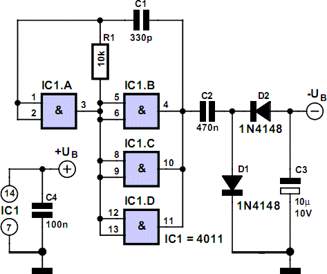
Some circuits need a negative supply voltage that only has to supply a small current. Providing a separate transformer winding for this (possibly even with a rectifier and filter capacitor) would be a rather extravagant solution. It can also be done using a few gates and several passive components. The combination of gate IC1a and the other three gates (wired in parallel) forms a square-wave generator. D1 and D2 convert the ac voltage into a dc voltage. As a CMOS IC is used here, the load on the negative output is limited to a few milliampères, depending on the positive supply voltage (see chart), despite the fact that three gates are connected in parallel.

However, as the figure shows, the negative voltage has almost the same magnitude as the positive input voltage, but with the opposite sign. If a clock signal in the range of 10–50 kHz is available, it can be connected to the input of IC1a, and R1 and C1 can then be omitted.

Negative Auxiliary Voltage circuit schematic

Polarity Reverser

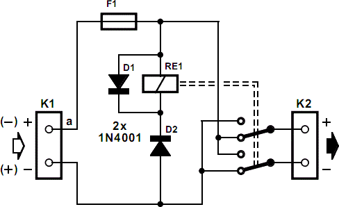
There are systems in which it is imperative that the supply voltage of, say, a motor, always has the correct polarity. It is, of course, possible to use a bridge rectifier for this, but if large currents are involved, this is not always possible. This may be because large voltage drops across diodes result in appreciable heat dissipation, or that the peak current exceeds the current rating of a diode. Fortunately, a good, inexpensive mechanical rectifier may be constructed with the aid of a relay. In the diagram, the supply voltage is applied to K1, while the motor that needs a supply with correct polarity is linked to K2. Provided fuse F1 is intact, a positive potential at terminal a of K1 will be applied to the positive terminal of K2. Diode D2 prevents the relay being energized.


When the polarity at K1 is reversed, the relay will be energized via D2. The relay contacts then interchange the connections to the terminals of K2 to ensure that the previous polarity of the supply to the load is retained. Diode D1 is a freewheeling diode for the relay coil. The type of relay to be used depends on the requisite operating voltage and the current through its contacts. Other parts of the circuit are not critical. It stands to reason that the circuit is not suitable for use with a small battery, since the relay coil draws a fairly large current

555 DC/DC Converter

It is all too often necessary to augment the power supply of an existing electronic circuit because exactly the voltage that you need is missing. The circuit presented here may provide a solution in a number of cases, since it can be used to convert a single-ended supply voltage into a balanced set of supply voltages. That’s not so remarkable by itself, but the special feature of this circuit is that this is accomplished without using difficult to obtain, exotic ICs. All of the components used in the circuit are ones that every electronics hobbyist is likely to have in a drawer somewhere.

The heart of the circuit is formed by an ‘old reliable’ 555 timer, which is wired here as a free-running oscillator with a frequency of approximately 160 kHz. The oscillator is followed by two voltage-doubling rectifiers, consisting of C1, D1, D2, C3 and C7, D3, D4, C5. They are followed in turn by two voltage regulators to stabilise the positive and negative voltages generated in this manner. The duty cycle of the 555 is set to approximately 50 percent using R1 and R2. The square-wave signal at the output of the timer IC has a DC offset, which is eliminated by C4 and R3.

The amplitude of the output signal from the 555 is approximately equal to the supply voltage less 1.5 V, so with a 12-V input voltage, there will be a square-wave signal on pin 3 with an amplitude of approximately 10.5 Vpp. With respect to ground (across R3), this is this +5 V / –5 V. Although this yields a symmetric voltage, its positive and negative amplitudes are somewhat too small and it is not stabilised. In order to split the square-wave signal into sufficiently large positive and negative amplitudes, C1/D2 are added for the positive voltage, causing the positive half to be doubled in amplitude.

For the negative half, the same effect is achieved using C7/D3. Following this, the two signals are smoothed by D1/C3 and D4/C5, respectively. Both voltages are now high enough to be input to normal 5-V voltage regulators, yielding symmetric +5V and –5V supply voltages at the output. The input voltage does not have to be regulated, although it must lie between +11 V and +18 V. The maximum output current is ±50 mA with an input voltage of 12 V. This circuit is an excellent choice for generating auxiliary voltages, such as supply voltages for low-power opamps. Naturally, the fact that the converter can be powered from the in-vehicle voltage of a car is a rather attractive feature.

Floating 9V Supply For DVM Modules

Most commercial DVM modules with an LCD readout are 9-V powered and based on an ICL7106 or similar A-D converter chip. These modules are typically used in laboratory power supplies and other test and measurement equipment where a drop-in solution needs to be found to realize a voltmeter readout. Particularly in power supply units, the LCD module will need to ‘float’ relative to the PSU supply rails, and this inevitably requires a separate 9-volt power supply. In some cases, batteries may be used but these have distinct advantages. The alternative, a 9-V converter effectively powered by the PSU and yet floating, is shown here.

It is built from the ubiquitous TLC555, LMC555 or 7555) timer IC acting in astable multivibrator configuration producing a 70-kHz square wave fed into a simple rectifier. In essence, capacitors C5 and C6 afford the above mentioned electrical isolation between the PSU supply rails and the LCD module. The old, bipolar NE555 IC should not be used here because it presents a too heavy loads on the converter’s own supply voltage. Depending on the exact type and brand of the CMOS 555 you’re using, resistor R6 may need to be redimensioned a bit to ensure a supply voltage of about 10 volts at pins 8 and 4 of the chip. At an output voltage of 9.5 V, the maximum output current of the converter s about 1 mA.

Adjustable 3 Ampere Regulator

By combining a common 78L05 with an integrated audio amplifier of the type TDA2030, an adjustable voltage regulator can be constructed in a very simple manner that works very well. The output voltage is adjustable up to 20 V, with a maximum current of 3 A. Since the TDA2030 comes complete with a good thermal and short-circuit protection circuit, this adjustable regulator is also very robust. As illustrated by the schematic, the design of this circuit is characterized by simplicity that is hard to beat. In addition to the two ICs, the regulator contains actually only two potentiometers and a few capacitors.

The adjustment is done by first turning potentiometer P1 to maximum (wiper to the side of the 78L05) and subsequently turning trimpot P2 until the desired maximum output voltage is reached. P1 is then used to provide a continuously adjustable voltage between this maximum and nearly zero volts. At relatively small output currents there are no specific requirements regarding the cooling. However, when the output current exceeds 1 A, or if the input to output voltage difference is quite large, the amplifier IC has to dissipate too much power and a small heatsink is certainly appropriate.

DC/DC Converter From +1.5V To +34V

An interesting DC/DC converter IC is available from Linear Technology. The LT1615 step-up switching voltage regulator can generate an output voltage of up to +34V from a +1.2 to +15V supply, using only a few external components. The tiny 5-pin SOT23 package makes for very compact construction. This IC can for example be used to generate the high voltage needed for an LCD screen, the tuning voltage for a varicap diode and so on. The internal circuit diagram of the LT1615 is shown in Figure 1. It contains a monostable with a pulse time of 400 ns, which determines the off time of the transistor switch.

If the voltage sampled at the feedback input drops below the reference threshold level of 1.23 V, the transistor switches on and the current in the coil starts to increase. This builds up energy in the magnetic field of the coil. When the current through the coil reaches 350 mA, the monostable is triggered and switches the transistor off for the following 400 ns. Since the energy stored in the coil must go somewhere, current continues to flow through the coil, but it decreases linearly. This current charges the output capacitor via the Schottky diode (SS24, 40V/2A). As long as the voltage at FB remains higher than 1.23V, nothing else happens.

DC/DC Converter From +1.5V To +34VAs soon as it drops below this level, however, the whole cycle is repeated. The hysteresis at the FB input is 8mV. The output voltage can be calculated using the formula Vout = 1.23V (R1+R2) / R2 The value of R1 can be selected in the megohm range, since the current into the FB input is only a few tens of nano-amperes. When the supply voltage is switched on, or if the output is short-circuited, the IC enters the power-up mode. As long as the voltage at FB is less than 0.6V, the LT1615 output current is limited to 250mA instead of 350mA, and the monostable time is increased to 1.5µs.

These measures reduce the power dissipation in the coil and diode while the output voltage is rising. In order to minimize the noise voltages produced when the coil is switched, the IC must be properly decoupled by capacitors at the input and output. The series resistance of these capacitors should be as low as possible, so that they can short noise voltages to earth. They should be located as close to the IC as possible, and connected directly to the earth plane. The area of the track at the switch output (SW) should be as small as possible. Connecting a 4.7-µF capacitor across the upper feedback capacitor helps to reduce the level of the output ripple voltage.

DC/DC Converter From +1.5V To +34VThe selection of the coil inductance is described in detail in the LT1615 data sheet at www.linear-tech.com. Normally, a 4.7µH filter choke is satisfactory for output voltages less than 7V. For higher voltages, a 10-µH choke should be used. In the data sheet, the Coilcraft DO1608-472 (4.7 µF) and DO1608-100 (10 µF) are recommended. The Schottky diode must naturally have a reverse blocking voltage that is significantly greater than the value of the output voltage. The types MBR0530 and SS24 are recommended. The shutdown input (/SHDN) can be used to disable the step-up regulator by applying a voltage that is less than +0.25V.

If the voltage at this pin is +0.9 V or higher, the LT1615 is active. You must bear in mind that even when the IC is disabled, the input voltage still can reach the output via the coil and the diode, reduced only by the forward voltage drop of the diode. The second circuit diagram for the LT1615 (Figure 2) shows how you can make a symmetric power supply using this switching regulator. Here the switch output of the IC is tapped off and rectified using a symmetrical rectifier. The voltage divider at the positive output of the rectifier determines the output voltage.