Tampilkan postingan dengan label Pulse_Freq Oscillator. Tampilkan semua postingan

Kamis, 10 Januari 2013

Mini Audio Signal Generator

A small audio test generator is very useful for quickly tracing a signal through an audio unit. Its main purpose is speed rather than refinement. A single sine-wave signal of about 1 kHz is normally all that is needed: distortion is not terribly important. It is, however, important that the unit does not draw too high a current. The generator described meets these modest requirements. It uses standard components, produces a signal of 899 Hz at an output level of 1 V r.m.s. and draws a current of only 20 µA. In theory, the low current drain would give a 9 V battery a life of 25,000 hours. The circuit is a traditional Wien bridge oscillator based on a Type TLC271 op amp. The frequency determining bridge is formed by C1, C2 and R1–R4. The two inputs of the op amp are held at half the supply voltage by dividers R3-R4 and R5-R6 respectively.

Resistors R5 and R6 also form part of the feedback loop. The amplification is set to about ´3 with P1. Diodes D1 and D2 are peak limiters. Since the limiting is based on the non-linearity of the diodes, there is a certain amount of distortion. At the nominal output voltage of 1 V r.m.s., the distortion is about 10%. This is, however, of no consequence in fast tests. Nevertheless, if 10% is considered too high, it may be improved appreciably by linking pin 8 of IC1 to ground. This increases the current drain of the circuit to 640 µA, but the distortion is down to 0.7%, provided the circuit is adjusted properly. If a distortion meter or similar is not available, simply adjust the output to 1 V r.m.s. Since the distortion of the unit is not measured in hundredths of a per cent, C1 and C2 may be ceramic types without much detriment. 

Sabtu, 29 Desember 2012

Simple Function Generator

Simple triangle-wave generators have a weakness in that the waveform of their output signal normally cannot be modified. The circuit presented here makes it possible to smoothly alter the waveform of a linearly rising and steeply trailing saw-tooth signal through a symmetrical triangle-wave to a slowly trailing, steeply rising linear sawtooth. The wanted waveform may be selected independently of the frequency, which can also be varied uniformly from 0.2 Hz to 8 kHz. At the same time, a rectangular signal with variable duty cycle (also independent of frequency) is available at the rectangular-signal output of the circuit.

The circuit consists of integrator IC1b, whose output is applied to comparator IC1c. The output of the comparator is a rectangular signal The output of IC1b is raised by amplifier IC1d to a level that allows the full output voltage range of the operational amplifier to be used. Op amp IC1a provides a stable virtual earth, whose level is set to half the supply voltage with P1. The smooth setting of the frequency is made possible by feedback of part of the output of the comparator to the input of the integrator via P2. This preset is usually not provided in standard triangle-wave generators. Network D1-R1-D2-R2-P3 makes it possible to give integrator capacitor C3 different charging and discharge times.

This arrangement enables the output signal at A1 and the duty cycle of the rectangular wave signal at A2 to be varied. Varying the amplification factor with P5 has no effect on the frequency set with P2. The slope of the signal edges, the transient responses, and the output voltage range (rail-to-rail or with some voltage drop) depend on the type of op amp used. The TL084 used in the prototype offers a good compromise between price and meeting the wanted parameters. The circuit is best built on a small piece of prototyping board. The circuit draws a current of not more than 12 mA.

Brief parameters:
Provides triangle-wave, sawtooth or rectangular signal
Waveform variable independently of frequency (triangle wave and sawtooth)
Duty cycle of rectangular signal can be set independently of frequency

Applications:
Test and measurement
Pulse-width control

Summary of preset action:
P1 – sets virtual earth to a level equal to Ucc/2;
P2 – sets the frequency;
P3– sets the waveform;
P4 – sets the hysteresis of the comparator (frequency and amplitude of the triangle-wave signal)
P5 – sets the amplification of the triangle-wave and sawtooth signals.

Selasa, 11 Desember 2012

Long-Interval Pulse Generator

A rectangular-wave pulse generator with an extremely long period can be built using only two components: a National Semiconductor LM3710 supervisor IC and a 100-nF capacitor to eliminate noise spikes. This circuit utilises the watchdog and reset timers in the LM3710. The watchdog timer is reset when an edge appears on the WDI input (pin 4). If WDI is continuously held at ground level, there are not any edges and the watchdog times out. After an interval TB, it triggers a reset pulse with a duration TA and is reloaded with its initial value. The cycle then starts all over again. As a result, pulses with a period of TA + TB are present at the RESET output (pin 10).


As can be seen from the table, periods ranging up to around 30 seconds can be achieved in this manner. The two intervals TA and TB are determined by internal timers in the IC, which is available in various versions with four different ranges for each timer. To obtain the desired period, you must order the appropriate version of the LM3710. The type designation is decoded in the accompanying table. The reset threshold voltage is irrelevant for this particular application of the LM3710. The versions shown in bold face were available at the time of printing. Current information can be found on the manufacturer’s home page (www.national.com). The numbers in brackets indicate the minimum and maximum values of intervals TA and TB for which the LM3710 is tested. The circuit operates with a supply voltage in the range of 3–5 V.

Optical Pulse Generator

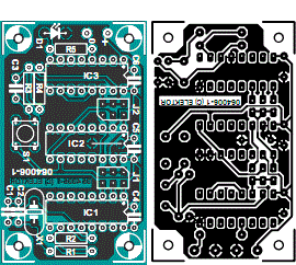
This little aid was originally designed to test the Shutter Time Meter. This meter was specifically designed for ‘analogue’ SLR cameras. In order to measure the exposure time of a camera accurately, it will first have to be checked with a well-defined signal first. This circuit was designed for that purpose. But the circuit can also be used if you need a well-defined pulse for some other purpose. The circuit is build around a trio of standard logic ICs. Firstly a 74HC4060 (IC1) is used to provide a quartz crystal accurate reference for the duration of the pulses. For the crystal frequency we choose the common 4.096 MHz value.


To test all the ranges of the shutter time meter, we choose three different pulse lengths in three different decades, namely: 1 / 2 / 4 / 10 / 20 / 40 / 100 / 200 / 400 ms. With jumper J1 you select a frequency of 1000, 500 or 250 Hz (see table). The frequency is then passed on to J2 and the dual decade counter IC2 (a 4518). This does not need to be a fast HC-type, since the frequency is at most 1 kHz. With J2 the frequency can be reduced by 1, 10 or 100 times. This frequency is then applied to IC3 (a 5-stage Johnson-counter). This has been set up in such a way that in the end there appears only one single pulse at the output.


The advantage of the Johnson-counter is that each output is free from glitches and has a duration that is exactly equal to the period of the clock input. We choose Q2 as the output. Q4 is used to stop the counter. Q0 is only active if we push the reset-button S1. IC3 will then start to count. To ensure that the reset does not affect the duration of the pulse, a differentiating RC-network R4/C3 generates a short reset pulse. R3 ensures that C4 is discharged after releasing S1. Also, just to be sure, we don’t use the second counter output but use the third one instead. For the same reason, to stop the counter we use the fifth output.
 

Especially with longer times you will notice that the pulse will arrive at the output a short time after pressing the switch. R5 drives a current of nearly 20 mA through D1. D1 provides sufficient light for this application to trigger the receiver diode in the shutter time meter. An unusually fast type was selected for the LED, which, with a switching time of 40 ns, has practically no influence on the length of the pulse. If you would like to use another LED then you will have to look closely at the switching time.


This needs to be small compared to the duration of the pulse. If you want to use the circuit with a logic level output then you can just omit D1. If necessary, the pulse lengths can be changed be selecting another crystal frequency. The current consumption in the idle state is less than 2 mA. In our prototype, while the circuit is delivering a pulse, the current consumption increases briefly to about 18 mA. Do not forget the wire link under IC2 when assembling the circuit.

Resistors
R1 = 1k
R2,R3 = 1M
R4 = 10k
R5 = 180
Capacitors
C1,C2 = 33pF
C3 = 10nF
C4,C5,C6 = 100nF ceramic, lead pitch 5mm
Semiconductors
D1 = HSDL-4230
IC1 = 74HC4060
IC2 = 4518
IC3 = 74HC4017
Miscellaneous
S1 = pushbutton, make contact, 6mm
J1,J2 = 3-way pinheader with jumper
X1 = 4.096MHz quartz crystal 1 wire link.

CMOS Crystal Frequency Multiplier

Crystals usually operate at fundamental frequencies up to about 15 MHz. Whenever higher frequencies are required a frequency multiplier is placed after the crystal oscillator. The resulting output signal is then a whole multiple of the crystal frequency. Other frequency multipliers often use transistors, which produce harmonics due to their non-linearity. These are subsequently filtered from the signal. One way of doing this is to put a parallel L-C filter in the collector arm. This filter could then be tuned to three times the input frequency. A disadvantage is that such a circuit would quickly become quite substantial.

This circuit contains only a single IC and a handful of passive components, and has a complete oscillator and two frequency triplers. The output is therefore a signal with a frequency that is 9 times as much as that of the crystal. Two gates from IC1, which contains six high-speed CMOS inverters, are used as an oscillator in combination with X1. This works at the fundamental frequency of the crystal and has a square wave at its output. A square wave can be considered as the sum of a fundamental sine wave plus an infinite number of odd multiples of that wave. The second stage has been tuned to the first odd multiple (3 x).


We know that some of our readers will have noticed that the filter used here is a band-rejection (series LC) type. Worse still, when you calculate the rejection frequency you’ll find that it is equal to the fundamental crystal frequency! The fundamental frequency is therefore attenuated, which is good. But how is the third harmonic boosted? That is done by the smaller capacitor of 33 pF in combination with the inductor. Together they form the required band-pass filter. (The same applies to the 12 pF capacitor in the next stage.) Through the careful selection of components, this filter is therefore capable of rejecting the fundamental and boosting the third harmonic! Clever, isn’t it?.
 
The output in this example is a signal of 30 MHz. The inverter following this stage heavily amplifies this signal and turns it into a square wave. The same trick is used again to create the final output signal of 3 times 30 MHz = 90 MHz. At 5 V this circuit delivers about 20 milliwatt into 50 R. This corresponds to +13 dBm and is in theory enough to drive a diode-ring balanced mixer directly. The circuit can be used for any output frequency up to about 100 MHz by varying the component values. When, for example, an 8 MHz crystal is used to obtain an output frequency of 72 MHz (9 x 8 = 72), the frequency determining inductors and capacitors have to be adjusted by a factor of 10/8.

You should round the values to the nearest value from the E12 series. Another application is for use in an FM transmitter; if you connect a varicap in series with the crystal, you can make an FM modulator. An added bonus here is that the relatively small modulation level is also increased by a factor of 9. Crystals with frequencies near 10 MHz are relatively easy to find and inexpensive, so you should always be able to find a suitable frequency within the FM band. A crystal of 10.245 MHz for instance would give you a frequency of 92.205 MHz and 10.700 MHz results in an output of 96.300 MHz. You may find that the circuit operates on the border of the HC specifications. If this causes any problems you should increase the supply voltage a little to 6V.


Pulse Frequency Modulator

The pulse width of the compact pulse cum frequency modulator can be varied by altering the change-over point of comparator IC1 with a control voltage via resistor R1. The hysteresis of the IC is determined by resistors R3 and R4. The control voltage also causes the frequency of the present circuit to be altered. When the input voltage is 0 V, the frequency is a maximum: in the present design this is about 3.8 kHz. The level of the output voltage is ±12–13 V. The more the change-over point has been shifted with the control voltage, the longer it will take before the potential across capacitor C1 has reached the level at which IC1 is enabled.

When the control voltage is larger than the zener voltage, the oscillator ceases to work. The maximum period is 25 ms, which may be adapted by altering the value of C1. This will, of course, also alter the maximum frequency. The duty cycle is inversely proportional to the control voltage. The minimum pulse width attainable at the lowest frequency is about 6 µs. The modulator draws a current not exceeding 5 mA.

1kH Synthetic Inductor

Inductors can be mimicked quite easily using operational amplifiers. The circuit shown here was developed to have an inductance of 1000 H (say, one thousand Henry) with good damping. Using this design you can build a resonant circuit with a center frequency of less than 1 Hz. The slow behavior allows you to use conventional measuring instruments to investigate the circuit in real time. The circuit can also be used as part of a filter design. Opamp1 operates as an Integrator, Opamp2 as a difference amplifier.

The output voltage of Opamp2 is equal to the voltage drop across R1 and P1, which is proportional to the output current. This voltage is differentiated by Opamp1, C1 and R2. The net effect is that the circuit behaves as an inductor. P1 allows adjustment of the inductance value. P2 allows adjustment of the Q factor of the coil by altering the symmetry of the difference amplifier and with it the stability of the circuit

10 to 1000 MHz Oscillator

Nowadays, it is no longer necessary to use discrete components to build oscillators. Instead, many manufacturers provide ready-made voltage-controlled oscillator (VCO) ICs that need only a few frequency-determining external components. One example is the RF Micro Devices RF2506. This IC operates with a supply voltage between 2.7 and 3.6 V (3.3V nominal) and provides a low-noise oscillator transistor with integrated DC bias setting. In addition, it has an isolating buffer amplifier that strongly reduces the effects of load variations (load pulling) on the oscillator. If a voltage less than 0.7V is applied to the power-down input (pin 8), the oscillator is shut down and the current consumption drops from 9mA to less than 1µA. The VCO is enabled when the voltage on pin 8 is at least +3V.


Connecting the feedback capacitors C1 and C2 to pins 3 (FDBK) and 4 (VTUNE) transforms the internal transistor into a Colpitts oscillator. A resonator is also needed; here this consists of C4 and L1, and it is coupled via C3. Keep the Q factor of the coil as high as possible (by using an air-core coil, for example), to ensure a low level of phase noise. Since most applications require a tuneable oscillator, the varicap diode D1 (BBY40, BBY51, BB804 etc) can be used to adjust the resonant frequency. The tuning voltage UTune is applied via a high resistance. The value of the tuning voltage naturally depends on the desired frequency range and the variable-capacitance diode (D1) that is used. The table shows a number of suggestions for selecting the frequency-determining components. If the frequency range is narrow, a parallel-resonant circuit should be connected between the output pin and +Vcc, to form the collector load for the output transistor.

10 to 1000 MHz Oscillator This can be built using the same components as the oscillator resonator. With a broadband VCO, use a HF choke instead, with a value of a few microhenries to a few nanohenries, depending on the frequency band. In this case C6 is not needed. The output level of this circuit is –3dBm with an LC load and –7 dBm with a choke load. The table that accompanies the schematic diagram provides rough indications of component values for various frequencies. It is intended to provide a starting point for experimentation. The coupling between the variable-capacitance diode and C5 determines the tuning range of the VCO. The manufacturer maintains an Internet site at www.rfmd.com, where you can find more information about this interesting oscillator IC.

Minggu, 18 November 2012

Low Frequency Sinewave Generators


The two circuits below illustrate generating low frequency sinewaves by shifting the phase of the signal through an RC network so that oscillation occurs where the total phase shift is 360 degrees. The transistor circuit on the right produces a reasonable sinewave at the collector of the 3904 which is buffered by the JFET to yield a low impedance output. The circuit gain is critical for low distortion and you may need to adjust the 500 ohm resistor to achieve a stable waveform with minimum distortion. The transistor circuit is not recommended for practical applications due to the critical adjustments needed. 

The op-amp based phase shift oscillator is much more stable than the single transistor version since the gain can be set higher than needed to sustain oscillation and the output is taken from the RC network which filters out most of the harmonic distortion. The sinewave output from the RC network is buffered and the amplitude restored by the second (top) op-amp which has gain of around 28dB. Frequency is around 600 Hz for RC values shown (7.5K and 0.1uF) and can be reduced by proportionally increasing the network resistors (7.5K). The 7.5K value at pin 2 of the op-amp controls the oscillator circuit gain and is selected so that the output at pin 1 is slightly clipped at the positive and negative peaks. The sinewave output at pin 7 is about 5 volts p-p using a 12 volt supply and appears very clean on a scope since the RC network filters out most all distortion occurring at pin 1.

Generating Long Time Delays


Generating long delays of several hours can be accomplished by using a low frequency oscillator and a binary counter as shown below. A single Schmitt Trigger inverter stage (1/6 of 74HC14) is used as a squarewave oscillator to produce a low frequency of about 0.5 Hertz. The 10K resistor in series with the input (pin 1) reduces the capacitor discharge current through the inverter input internal protection diodes if the circuit is suddenly disconnected from the supply. This resistor may not be needed but is a good idea to use. The frequency is divided by two at each successive stage of the 12 stage binary counter (CD4040) which yields about 1 hour of time before the final stage (Q12) switches to a high state. Longer or shorter times can be obtained by adjusting the oscillator frequency or using different RC values. Each successive stage changes state when the preceding stage switches to a low state (0 volts), thus the frequency at each stage is one half the frequency of the stage before. Waveform diagrams are shown for the last 3 stages. To begin the delay cycle, the counter can be reset to zero by momentarily connecting the reset line (pin 11) to the positive supply. Timing accuracy will not be as good as with a crystal oscillator and may only be around 1 or 2% depending on the stability of the oscillator capacitor.

Monostable Flip Flop


The monostable flip flop, sometimes called a 'one shot' is used to produce a single pulse each time it is triggered. It can be used to debounce a mechanical switch so that only one rising and one falling edge occurs for each switch closure, or to produce a delay for timing applications. In the discrete circuit, the left transistor normally conducts while the right side is turned off. Pressing the switch grounds the base of the conducting transistor causing it to turn off which causes the collector voltage to rise. As the collector voltage rises, the capacitor begins to charge through the base of the opposite transistor, causing it to switch on and produce a low state at the output. The low output state holds the left transistor off until the capacitor current falls below what is needed to keep the output stage saturated. When the output side begins to turn off, the rising voltage causes the left transistor to return to it's conducting state which lowers the voltage at it's collector and causes the capacitor to discharge through the 10K resistor (emitter to base). The circuit then remains in a stable state until the next input. The one shot circuit on the right employs two logic inverters which are connected by the timing capacitor. When the switch is closed or the input goes negative, the capacitor will charge through the resistor generating an initial high level at the input to the second inverter which produces a low output state. The low output state is connected back to the input through a diode which maintains a low input after the switch has opened until the voltage falls below 1/2 Vcc at pin 3 at which time the output and input return to a high state. The capacitor then discharges through the resistor (R) and the circuit remains in a stable state until the next input arrives. The 10K resistor in series with the inverter input (pin 3) reduces the discharge current through the input protection diodes. This resistor may not be needed with smaller capacitor values.
Note: These circuits are not re-triggerable and the output duration will be shorter than normal if the circuit is triggered before the timing capacitors have discharged which requires about the same amount of time as the output. For re-triggerable circuits, the 555 timer, or the 74123 (TTL), or the 74HC123 (CMOS) circuits can be used.

Bistable Flip Flop

Here are two examples of bistable flip flops which can be toggled between states with a single push button. When the button is pressed, the capacitor connected to the base of the conducting transistor will charge to a slightly higher voltage. When the button is released, the same capacitor will discharge back to the previous voltage causing the transistor to turn off. The rising voltage at the collector of the transistor that is turning off causes the opposite transistor to turn on and the circuit remains in a stable state until the next time the button is pressed and released. Note that in the LED circuit, the base current from the conducting transistor flows through the LED that should be off, causing it to illuminate dimly. The base current is around 1 mA and adding a 1K resistor in parallel with the LED will reduce the voltage to about 1 volt which should be low enough to ensure the LED turns completely off.

Triangle and Squarewave Generator

Here is a simple triangle/squarewave generator using a common 1458 dual op-amp that can be used from very low frequencies to about 10 Khz. The time interval for one half cycle is about R*C and the outputs will supply about 10 milliamps of current. Triangle amplitude can be altered by adjusting the 47K resistor, and waveform offset can be removed by adding a capacitor in series with the output.

Low Frequency Wien Bridge RC Sinewave Oscillators