Tampilkan postingan dengan label Audio Power HI FI. Tampilkan semua postingan

Kamis, 10 Januari 2013

A Hiqh Quality Headphone Amplifier

Low distortion Class-B circuitry, 6V Battery Operated


Some lovers of High Fidelity headphone listening prefer the use of battery powered headphone amplifiers, not only for portable units but also for home "table" applications. This design is intended to fulfill their needs. An improved output driving capability is gained by making this a push-pull Class-B arrangement. Output power can reach 100mW RMS into a 16 Ohm load at 6V supply with low standing and mean current consumption, allowing long battery duration.


 Parts:

Resistors:
P1 = 22K Potentiometer
R1 = 15K Resistor
R2 = 100K Resistor
R3 = 100K Resistor
R4 = 47K Resistor
R5 = 470R Resistor
R6 = 500R Resistor
R7 = 1K Resistor
R8 = 18K Resistor
R9 = 18K Resistor
R10 = 2.2R Resistor
R11 = 2.2R Resistor
R12 = 33R Resistor
R13 = 4.7K Resistor

Capacitors:
C1 = 10uF-25V Capacitors
C2 = 10uF-25V Capacitors
C3 = 100nF-63V (PF)
C4 = 220uF-25V Capacitors
C5 = 100nF-63V (PF)
C6 = 220uF-25V Capacitors

Semiconductors:
Q1 = BC560C PNP Transistor
Q2 = BC560C PNP Transistor
Q3 = BC550C NPN Transistor
Q4 = BC550C NPN Transistor
Q5 = BC560C PNP Transistor
Q6 = BC327 PNP Transistor
Q7 = BC337 NPN Transistor

Miscellaneous:
J1 = RCA Audio Input Socket
J2 = 3mm Stereo Jack Socket
B1 = 6V Battery Rechargeable
SW1=SPST Slide or Toggle Switch


Notes:
  • For a Stereo version of this circuit, all parts must be doubled except P1, SW1, J2 and B1.
  • Before setting quiescent current rotate the volume control P1 to the minimum, Trimmer R6 to maximum resistance and Trimmer R3 to about the middle of its travel.
  • Connect a suitable headphone set or, better, a 33 Ohm 1/2W resistor to the amplifier output.
  • Switch on the supply and measure the battery voltage with a Multimeter set to about 10Vdc fsd.
  • Connect the Multimeter across the positive end of C4 and the negative ground.
  • Rotate R3 in order to read on the Multimeter display exactly half of the battery voltage previously measured.
  • Switch off the supply, disconnect the Multimeter and reconnect it, set to measure about 10mA fsd, in series to the positive supply of the amplifier.
  • Switch on the supply and rotate R6 slowly until a reading of about 3mA is displayed.
  • Check again the voltage at the positive end of C4 and readjust R3 if necessary.
  • Wait about 15 minutes, watch if the current is varying and readjust if necessary.
  • Those lucky enough to reach an oscilloscope and a 1 KHz sine wave generator can drive the amplifier to the maximum output power and adjust R3 in order to obtain a symmetrical clipping of the sine wave displayed.


Technical data:

Output power (1 KHz sine wave):
  • 16 Ohm: 100mW RMS
  • 32 Ohm: 60mW RMS
  • 64 Ohm: 35mW RMS
  • 100 Ohm: 22.5mW RMS
  • 300 Ohm: 8.5mW RMS
Sensitivity:
  • 160mV input for 1V RMS output into 32 Ohm load (31mW)
  • 200mV input for 1.27V RMS output into 32 Ohm load (50mW)
Frequency response @ 1V RMS:
  • Flat from 45Hz to 20 KHz, -1dB @ 35Hz, -2dB @ 24Hz
Total harmonic distortion into 16 Ohm load @ 1 KHz:
  • 1V RMS (62mW) 0.015% 1.27V RMS (onset of clipping, 100mW) 0.04%
Total harmonic distortion into 16 Ohm load @ 10 KHz:
  • 1V RMS (62mW) 0.05% 1.27V RMS (onset of clipping, 100mW) 0.1%
  • Unconditionally stable on capacitive loads

USB Powered Audio Power Amplifier

This circuit of multimedia speakers for PCs has single-chip-based design, low-voltage power supply, compatibility with USB power, easy heat-sinking, low cost, high flexibility and wide temperature tolerance. At the heart of the circuit is IC TDA2822M. This IC is, in fact, mono-lithic type in 8-lead mini DIP package. It is intended for use as a dual audio power amplifier in battery-powered sound players.

Specifications of TDA2822M are low quiescent current, low crossover distortion, supply voltage down to 1.8 volts and minimum output power of around 450 mW/channel with 4-ohm loudspeaker at 5V DC supply input. An ideal power amplifier can be simply defined as a circuit that can deliver audio power into external loads without generating significant signal distortion and without consuming excessive quiescent current.

This circuit is powered by 5V DC supply available from the USB port of the PC. When power switch S1 is flipped to ‘on’ position, 5V power supply is extended to the circuit and power-indicator red LED1 lights up instantly. Resistor R1 is a current surge limiter and capacitors C1 and C4 act as buffers. Working of the circuit is simple. Audio signals from the PC audio socket/headphone socket are fed to the amplifier circuit through components R2 and C2 (left channel), and R3 and C3 (right channel).


Potmeter VR1 works as the volume controller for left (L) channel and potmeter VR2 works for right (R) channel. Pin 7 of TDA2822M receives the left-channel sound signals and pin 6 receives the right-channel signals through VR1 and VR2, respectively. Ampl i f ied signals for driving the left and right loudspeakers are available at pins 1 and 3 of IC1, respectively. Components R5 and C8, and R6 and C10 form the traditional zobel network.

Assemble the circuit on a medium-size, general-purpose PCB and enclose in a suitable cabinet. It is advisable to use a socket for IC TDA2822M. The external connections should be made using suitably screened wires for better result.

High Power Headphone Amplifier Using BD139-40

Firstly, I'd like to stress that the intended use of this circuit is only one of many possible applications. Apart from the obvious usage as a headphone amplifier, the circuit can be used for a range of applications where a wide bandwidth low power amplifier is needed. Some of the options include ...
  • Reverb drive amplifier - ideal for low and medium impedance reverb tanks
  • High current line driver - suitable for very long balanced lines
  • Low power speaker amplifier - better performance than small integrated amps
  • ... and of course, a headphone amp.
In short, the amp can be used anywhere that you need an opamp with more output current than normally available. Since most are rated for around ±20-50mA, general purpose opamps are not suitable for driving long cables or anywhere else that a relatively high output current is needed.

As a headphone amplifier, this design is very similar to others on the ESP site, but the main difference is that this one (and P70) has been built and fully tested. The design is fairly standard, and every variation was checked out before arriving at the final circuit. A photo of the prototype is shown below, and at only 64 x 38mm (2.5 x 1.5 inches) it is very small - naturally, the heatsink is not included in the dimensions.

The amplifier is capable of delivering around 1.5W into 8 ohm headphones, and 2.2W into 32 ohms - this is vastly more than will ever be needed in practice. The use of a 120 Ohm output resistor is recommended, as this is supposed to be the standard source impedance for headphones. Unfortunately, many users have found that their 'phones perform better when driven from a low impedance source.
 
 
The circuit is based on an opamp, with its output current boosted by a pair of transistors. Distortion is well below my measurement threshold at all levels below clipping into any impedance. Noise is virtually non-existent - even with a compression driver held to my ear, I could barely hear any, and I couldn't hear any with headphones.
 
 
 Construction

While it may be possible to build it using Veroboard or similar, there is a high risk that it will oscillate because of the very wide bandwidth of the amplifier. A capacitor may be added in parallel with R4 (L and R) to reduce the bandwidth if stability problems are encountered. Although I used an NE5532 opamp for the prototype, the circuit will also work with a TL072, but at reduced power. You may also substitute an OPA2134 or your favorite device, taking note of the following ...
opamp pinoutThe standard pinout for a dual opamp is shown on the left. If the opamps are installed backwards, they will almost certainly fail, so be careful.

The suggested NE5532 opamp was used for the prototype, and performance is exemplary. Devices such as the TL072 will be quite satisfactory for most work, but if you prefer to use ultra low noise or wide bandwidth devices, that choice is yours.

Construction is fairly critical. Because of the wide bandwidth of the NE5532 and many other audio grade opamps, the amplifier may oscillate (the prototype initially had an oscillation at almost 500kHz), so care is needed to ensure there is adequate separation between inputs and outputs. Even a small capacitive coupling between the two may be enough to cause problems.

As shown in the photo, this amplifier needs a heatsink. While it can operate without one at low power using high impedance headphones, you need to plan for all possibilities (after all, you may purchase low impedance 'phones sometime in the future). The heatsink does not need to be massive, and the one shown above is fine for normal listening levels. An aluminium bracket may be used to attach to the chassis - I recommend 3mm material. Note that the heatsink should always be earthed (grounded).

The output transistors must be insulated from the heatsink. Sil-Pads™ are quite suitable because of the relatively low dissipation, but greased mica or Kapton can be used if you prefer. If you use the suggested 3mm aluminium, you can drill and tap threads into the heatsink, removing the need for nuts.

Testing

Connect to a suitable power supply - remember that the supply earth (ground) must be connected! When powering up for the first time, use 56 ohm "safety" resistors in series with each supply to limit the current in case you have made a mistake in the wiring. These will reduce the supply voltage considerably because of the bias current of the output transistors.

If the voltage at the amplifier supply pins is greater than ±6V and the output voltage is close to zero, then the amplifier is probably working fine. If you have an oscilloscope, check for oscillation at the outputs ... at all volume control settings. Do this without connecting your headphones - if the amp oscillates, it may damage them.

Once you are sure that all is well, you may remove the safety resistors and permanently wire the amplifier into your chassis.

Audio Level Threshold Control

This circuit was originally designed for use in detecting discharges from individual neurons, where the infrequent discharges are difficult to separate from dominant background noise. It may also prove useful in other applications that need to detect infrequent low-level audio signals against a noisy background. The audio input signal is buffered by op amp IC1 before being applied to the opposing inputs of comparators IC4 & IC5. Positive and negative offset voltages are generated by VR1 and IC2 and fed to the other two inputs of the comparators. Essentially, the comparators act to produce a negative voltage at their commoned outputs (C) whenever the audio signal exceeds either the positive or negative offset voltage.


The signal at "C" is inverted by transistor Q1 to produce "D". These two signals are used to control a pair of CMOS switches (S1 & S2), which either pass the audio signal to the output or short it to ground. The signal from the CMOS switches is buffered by IC3, which in conjunction with the 10kΩ resistor and 10nF capacitor filters out the switching artefacts. In practice, the offset voltage is adjusted until there is little or no breakthrough of the noise background at the output. Thereafter, only audio signals exceeding the threshold are passed. Inevitably, this produces some crossover distortion but this is of little consequence compared with the benefit of the quiet background.

Guitar Control

Stand-alone, 9V battery powered unit, Three-level input selector, three-band tone control

This preamplifier was designed as a stand-alone portable unit, useful to control the signals generated by guitar pick-ups, particularly the contact "bug" types applied to acoustic instruments. Obviously it can be used with any type of instrument and pick-up. It features a -10dB, 0dB and +10dB pre-set input selector to adjust input sensitivity, in order to cope with almost any pick-up type and model. A very long battery life is ensured by the incredibly low current consumption of this circuit, i.e. less than 800µA.


Parts:

P1,P2_________100K Linear Potentiometers
P3____________470K Linear Potentiometer
P4_____________10K Log. Potentiometer
R1____________150K 1/4W Resistor
R2____________220K 1/4W Resistor
R3_____________56K 1/4W Resistor
R4____________470K 1/4W Resistor
R5,R6,R7_______12K 1/4W Resistors
R8,R9___________3K9 1/4W Resistors
R10,R11_________1K8 1/4W Resistors
R12,R13________22K 1/4W Resistors
C1____________220nF 63V Polyester Capacitor
C2,C8___________4µ7 63V Electrolytic Capacitors
C3_____________47nF 63V Polyester Capacitor
C4,C6___________4n7 63V Polyester Capacitors
C5_____________22nF 63V Polyester Capacitor
C7,C9_________100µF 25V Electrolytic Capacitors
IC1___________TL062 Low current BIFET Dual Op-Amp
J1,J2__________6.3mm. Mono Jack sockets
SW1______________1 pole 3 ways rotary or slider switch
SW2______________SPST Switch
B1_______________9V PP3 Battery Clip for PP3 Battery

Circuit operation:

IC1A op-amp is wired as an inverting amplifier, having its gain set by a three ways switch inserting different value resistors in parallel to R4. This input stage is followed by an active three-band tone control stage having unity gain when controls are set in their center position and built around IC1B.

Technical data:

Frequency response:
20Hz to 20KHz -0.5dB, controls flat.
Tone control frequency range:
±15dB @ 30Hz; ±19dB @ 1KHz; ±16dB @ 10KHz.
Maximum input voltage (controls flat):
900mV RMS @ +10dB input gain; 7.5V RMS @ -10dB input gain.
Maximum undistorted output voltage:
2.5V RMS.
Total Harmonic Distortion measured @ 2V RMS output:
<0.012% @ 1KHz; <0.03% @ 10KHz.
THD @ 1V RMS output:
less 0.01%
Total current drawing:
less 800µA.

Mini Audio Signal Generator

A small audio test generator is very useful for quickly tracing a signal through an audio unit. Its main purpose is speed rather than refinement. A single sine-wave signal of about 1 kHz is normally all that is needed: distortion is not terribly important. It is, however, important that the unit does not draw too high a current. The generator described meets these modest requirements. It uses standard components, produces a signal of 899 Hz at an output level of 1 V r.m.s. and draws a current of only 20 µA. In theory, the low current drain would give a 9 V battery a life of 25,000 hours. The circuit is a traditional Wien bridge oscillator based on a Type TLC271 op amp. The frequency determining bridge is formed by C1, C2 and R1–R4. The two inputs of the op amp are held at half the supply voltage by dividers R3-R4 and R5-R6 respectively.

Resistors R5 and R6 also form part of the feedback loop. The amplification is set to about ´3 with P1. Diodes D1 and D2 are peak limiters. Since the limiting is based on the non-linearity of the diodes, there is a certain amount of distortion. At the nominal output voltage of 1 V r.m.s., the distortion is about 10%. This is, however, of no consequence in fast tests. Nevertheless, if 10% is considered too high, it may be improved appreciably by linking pin 8 of IC1 to ground. This increases the current drain of the circuit to 640 µA, but the distortion is down to 0.7%, provided the circuit is adjusted properly. If a distortion meter or similar is not available, simply adjust the output to 1 V r.m.s. Since the distortion of the unit is not measured in hundredths of a per cent, C1 and C2 may be ceramic types without much detriment. 

Three Channel Audio Mixer Circuit

Three high/low-sensitivity switchable inputs


Although the modular Portable Mixer design available on these web pages has become a hit for many amateurs, some correspondents required a much simpler device, mainly for mixing mono signals. This design should fulfil their needs, featuring three inputs with switchable high/low sensitivity and unusual level-control circuits, providing high overload margins and low-noise figures, proportional to gain-level settings. Low current consumption due to a simple, five-transistor circuitry, allows the Mini Mixer to be powered by a common 9V PP3 battery for many hours.


Parts:

P1 = 5K
P2 = 5K
P3 = 5K
R1 = 180K
R2 = 2M2
R3 = 750R
R4 = 1K
R5 = 15K
R6 = 220R
R7 = 1.5K
R8 = 820R
R9 = 150R
R10 = 100K
R11 = 180K
R12 = 2.2M
R13 = 750R
R14 = 1K
R15 = 180K
R16 = 2M2
R17 = 750R
R18 = 1K

Capacitors:

C1 = 1µF-63V
C2 = 100µF-25V
C3 = 220µF-25V
C4 = 100µF-25V
C5 = 220µF-25V
C6 = 1µF-63V
C7 = 100µF-25V
C8 = 1µF-63V
C9 = 100µF-25V

Transistors:

Q1 = BC550C
Q2 = BC547
Q3 = BC557
Q4 = BC550C
Q5 = BC550C

Misc. Components

B1 = 9V PP3 Battery
J1,J2,J3 = 3mm Mono Jack sockets
SW1,2,3,4 = SPST Toggle or Slider Switches


Notes:
  • When SW1, SW2 or SW3 are open the input sensitivity is suited to high-output devices like CD players, tuners, tape recorders, iPods, miniDisc players, computer audio outputs etc.
  • When SW1, SW2 or SW3 are closed the input sensitivity is suited to low-output, low-impedance moving coil or electret microphones.
  • Sometimes, the 750 Ohm value for R3, R13 and R17 resistors could be not easy to find. In this case, two 1K5 resistors wired in parallel can be used to replace each item.
  • To make a stereo mixer, all the parts must be doubled excepting R6, C3, C5, SW4 and B1.

Digital Volume Control

Simple circuitry, Suitable for all kind of audio amplifiers


This circuit could be used for replacing your manual volume control in a stereo amplifier. In this circuit, push-to-on switch SW1 controls the forward (volume increase) operation of both channels while a similar switch SW2 controls reverse (volume decrease) operation of both channels. A readily available IC from Dallas semiconductor, DS1669 is used here.

Parts:

J1 = RCA Audio Input Socket
J2 = RCA Audio Input Socket
C1 = 0.1uF-16V Ceramic Disc Capacitor
C2 = 0.1uF-16V Ceramic Disc Capacitor
C3 = 0.1uF-16V Ceramic Disc Capacitor
IC1 = DS1669 (is available from Dallas SCo.
SW1 = Momentary Push Button Switch


Notes:
  • Replaces mechanical variable resistors.
  • Electronic interface provided for digital as well as manual control.
  • Wide differential input voltage range between 4.5 and 8 volts.
  • Wiper position is maintained in the absence of power.
  • Low-cost alternative to mechanical controls.
  • Applications include volume, tone, contrast, brightness, and dimmer control.
  • The circuit is extremely simple and compact requiring very few external components.
  • The power supply can vary from 4.5V to 8V.
  • The input signal should not fall below -0.2 volts.

Rabu, 02 Januari 2013

Bass Booster Circuit

Bass Boost is today's sound... whether it's the driving, gut-vibration pulsation of disco, or the solid bass line of soft, hard, or laid-back rock. One way to get the modern bass-boost sound without running out and buying an all-new expensive piece of equipment is to use a Bass Booster between your guitar, electronic organ or what-have-you, and the instrument amplifier. A bass booster strips the highs from the instrument's output signal and amplifies low frequencies, feeding on "all-bass" sound to the instrument amplifier. Naturally, the bigger the speaker used with the amp, the more powerful the bass: use 15-inchers with the Bass Booster and you can rattle the windows. Bass Booster is powered by an ordinary 9 volt transistor radio battery. It can be assembled on a small printed board or on a veroboard using point to point wiring. The booster connects between your instrument and its amplifier through two standard RCA Jacks.
 
 
Parts:

P1 = 50K
P2 = 100K
R1 = 22K
R2 = 470K
R3 = 47K
R4 = 10K
R5 = 470R
R6 = 1K
Q1 = 2N2222
C1 = 2.2uF-25v

C2 = 100nF-63v
C31 = 00nF-63V
C4 = 3.3uF-25v
C5 = 470uF-25v
D1 = 5mm. Red Led
Q1 = 2N2222
B1 = 9v Battery

J1 = RCA Audio Input Socket
J2 = RCA Audio Output Socket
S1 = On-Off Switch


Using Bass Booster:

Connect your electronic guitar or other electronic instrument to input jack J1; Connect output jack J2 to your instruments amplifier's normally-used input. With power switch S1 off, key S2 so the instrument feeds directly to the instrument amplifier. With P2 set full counter-clockwise (Off), turn power switch S1 on, key S2 once, and advance P2 for the desired Bass Boost level. To cut back to natural sound just stomp down on S2 and key the Bass Booster out. Don't worry about leaving power switch S1 on for several hours of a gig. The circuit pulls less than 1mA from the battery, so battery will last many, many months.

Audio Booster

The amplifier's gain is nominally 20 dB. Its frequency response is determined primarily by the value of just a few components-primarily C1 and R1. The values of the schematic diagram provide a response of ±3.0 dB from about 120 Hz to better than 20,000 Hz.Actually, the frequency response is ruler flat from about 170 Hz to well over 20,000 Hz; it's the low end that deviates from a flat frequency response. The low end's roll-off is primarily a function of capacitor C1(since RI's resistive value is fixed). If C1's value is changed to 0.1 pF, the low end's comer frequency-the frequency at which the low-end roll-off starts-is reduced to about 70 Hz. If you need an even deeper low-end roll-off, change C1 to a 1.0 pF capacitor; if it's an electrolytic type, make certain that it's installed into the circuit with the correct polarity, with the positive terminal connected to Q1's base terminal.


Parts:
P1 = 100K
R1 = 47K
R2 = 470K
R3 = 10K
R4 = 560R
R5 = 270R
C1 = 0.1uF-25v
C2 = 3.3uF-25v
C3 = 470uF-25V
D1 = 5mm. Red Led
B1 = 9v Battery
J1 = RCA Audio Input Socket
J2 = RCA Audio Output Socket
S1 = On-Off Switch

Selasa, 11 Desember 2012

Audio Amplifier Output Relay Delay " Speaker Protector "

This is a simple circuit which I built to one of my audio amplifier projects to control the speaker output relay. The purpose of this circuit is to control the relay which turns on the speaker output relay in the audio amplifier. The idea of the circuit is wait around 5 seconds ofter the power up until the speakers are switched to the amplifier output to avoid annoying "thump" sound from the speakers. Another feature of this circuit is that is disconnects the speaker immediately when the power in the amplifier is cut off, so avoiding sometimes nasty sounds when you turn the equipments off.

Component list
C1 = 100 uF 40V electrolytic
C2 = 100 uF 40V electrolytic
D1 = 1N4007
D2 = 1N4148
Q1 = BC547
R1 = 33 kohm 0.25W
R2 = 2.2 kohm 0.25W
RELAY 24V DC relay, coil resistance >300 ohm

Circuit operation:

Then power is applied to the power input of the circuit, the positive phase of AC voltage charges C1. Then C2 starts to charge slowly through R1. When the voltage in C2 rises, the emitter output voltage of Q1 rises together with voltage on C2. When the output voltage of Q2 is high enough (typically around 16..20V) the relay goes to on state and the relay witches connect the speakers to the amplifier output. It takes typically around 5 seconds after power up until the relay starts to conduct (at absolute time depends on the size of C2, relay voltage and circuit input voltage). When the power is switched off, C1 will loose it's energy quite quickly. Also C2 will be charged quite quickly through R2. In less than 0.5 seconds the speakers are disconnected from the amplifier output.

Notes on the circuit:
This circuit is not the most accurate and elegant design, but it has worked nicely in my small home-built PA amplifier. This circuit can be also used in many other applications where a turn on delay of few seconds is needed. The delay time can be increased by using bigger C2 and decreased by using a smaller C2 value. Note that the delay is not very accurate because of simplicity of this circuit and large tolerance of typical electrolytic capacitors (can be -20%..+50% in some capacitors).

Portable Microphone Preamplifier

This circuit is mainly intended to provide common home stereo amplifiers with a microphone input. The battery supply is a good compromise: in this manner the input circuit is free from mains low frequency hum pick-up and connection to the amplifier is more simple, due to the absence of mains cable and power supply. Using a stereo microphone the circuit must be doubled. In this case, two separate level controls are better than a dual-ganged stereo potentiometer. Low current drawing (about 2mA) ensures a long battery life.

 Parts:

P1 = 2.2K
R1 = 100K
R2 = 100K
R3 = 100K
R4 = 8.2K
R5 = 68R
R6 = 6.8K
R7 = 1K
R8 = 1K
R9 = 150R
C1 = 1uF-63V
C2 = 100uF-25V
C3 = 100uF-25V
C4 = 100uF-25V
C5 = 22uF-25V
Q1 = BC560
Q2 = BC550

Circuit Operation:

The circuit is based on a low noise, high gain two stage PNP and NPN transistor amplifier, using DC negative feedback through R6 to stabilize the working conditions quite precisely. Output level is attenuated by P1 but, at the same time, the stage gain is lowered due to the increased value of R5. This unusual connection of P1, helps in obtaining a high headroom input, allowing to cope with a wide range of input sources (0.2 to 200mV RMS for 1V RMS output).


Notes:
  • Harmonic distortion is about 0.1% @ 1V RMS output (all frequencies).
  • Maximum input voltage (level control cursor set at maximum) = 25mV RMS
  • Maximum input voltage (level control cursor set at center position) = 200mV RMS
  • Enclosing the circuit in a metal case is highly recommended.
  • Simply connect the output of this device to the Aux input of your amplifier through screened cable and suitable connectors.

Selasa, 27 November 2012

Paraphase Tone Controller

As opposed to the widespread Baxandall circuit (dating back to 1952!) a ‘paraphrase’ tone control supplies a straight frequency response as long as the bass and treble controls are in the same position. This unique property makes the ‘paraphase’ configuration of interest if only treble or bass needs to be adjusted - it is not possible to adjust both at the same time! Essentially, it’s the difference in setting of the tone controls that determines the slope of the frequency response, and the degree of bass/treble correction. The circuit is simplicity itself, based on two networks C1-C2-C3/R9-R10-R11 and C5-C6-C7/R12-R13-R14.

Paraphase Tone Controller Circuit Picture:
 
 
The first is for the high frequencies (treble) response, the second, for the low frequencies (bass). The roll-off points have been selected, in combination with C4 and C8, for the sum of the two output signals to re-appear with a ‘straight’ frequency response again at the output. Roughly equal output levels from the networks are ensured by R6 = 7.15 k and R8 = 6.80 k. However, the operating principle requires the input signals to the two networks to be in anti-phase. For best operation the networks are driven by two buffers providing some extra gain.
Paraphase Tone Controller Circuit diagram:
   
 
The gain of IC1.D is slightly higher than that of IC1.C to ensure the overall response curve remains as flat as possible at equal settings of the tone controls. Because each network introduces a loss of about 1.72 (times), IC1.D and IC1.C first amplify the signal. The gain is set at about 8 (times) allowing input signal levels up to 1 V to pass the circuit at maximum gain and distortion-free. The gain also compensates the attenuation if you prefer to keep the tone controls at the mid positions for a straight response.
Parts and PCB layout:
 
 
Parts and PCB Layout
To audio fans, the circuit is rewarding to experiment with, especially in respect of the crossover point of the two networks. R3 and R4 determine the control range, which may be increased (within limits) by using lower resistor values here. The values shown ensure a tone control range of about 20 dB. IC1.B buffers the summed signal across R15. C9 removes any DC-offset voltage and R16 protects the output buffer from the effects of too high capacitive loads. R17, finally, keeps the output at 0 V. The choice of the quad opamp is relatively uncritical. Here the unassuming TL074 is used but you may even apply rail to rail opamps as long as they are stable at unity gain. Also, watch the supply voltage range. A simple circuit board was designed for the project. Linear-law potentiometers may be fitted directly onto the board. Two boards are required for a stereo application. The relevant connections on the boards are then wired to a stereo control potentiometer.
Specification:
  • Current consumption (no signal) 8 mA
  • Max. input signal 1 Veff (at max. gain)
  • Gain at 20 Hz +13.1 dB max. –6.9 dB min.
  • at 20 kHz +12.2 dB max. –7.6 dB min
  • Gain (controls at mid position) 2.38 x
  • Distortion (1 Veff, 1 kHz) 0.002% (B = 22kHz) 0.005% (B = 80 kHz)
COMPONENTS LIST
Resistors
R1-R4 = 10k
R5,R7 = 1k
R6 = 7k15
R8 = 6k80
R9,R10,R11 = 8k2
R12,R13,R14 = 2k2
R15 = 1M
R16 = 100R
R17 = 100k
P1,P2 = 100k preset or chassis-
mount control potentiometer, linear law
Capacitors
C1,C2,C3 = 47nF MKT, lead pitch 5mm
C4 = 68nF MKT, lead pitch 5mm
C5,C6,C7 = 10nF MKT, lead pitch 5mm
C8,C10,C11 = 100nF MKT, lead pitch 5mm
C9 = 2µF2 MKT, lead pitch 5mm or 7.5mm
Semiconductors
IC1 = TL074
Miscellaneous
K1,K2 = line socket, PCB mount, e.g.
T-709G (Monacor/Monarch)

Balanced Output Board For The Stereo DAC

This add-on board is designed to provide a pair of balanced audio outputs for the High-Quality Stereo DAC (Digital to Analog Converter). Two 3-pin male XLR connectors are used for the new outputs and they can either replace or augment the existing unbalanced outputs without affecting their performance. Balanced audio is used in recording studios and on stage because of its improved noise immunity.

Picture of the project:
 
 
This is due to the fact that the signal is sent differentially (ie, as two signals 180° out of phase) and then converted to a single-ended voltage signal at the far end. If any noise is picked up in the cable, it affects the two out-of-phase signals equally so that when the signals are subsequently subtracted, most of the noise is eliminated.
Parts layout:


In addition, the DAC’s performance at the balanced outputs generally exceeds that of the unbalanced outputs, although only by a small margin. The signal-to-noise ratio, frequency response and channel separation are all better, although we measured a tiny bit more distortion from the balanced outputs. However, both levels are so low as to be almost negligible.

Circuit diagram:


Comparison chart:


Selasa, 20 November 2012

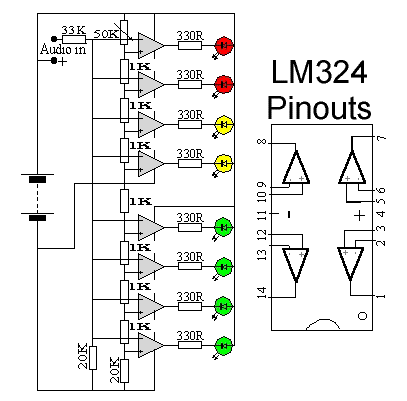
Audio VU Meter

Notes
The 1K resistors in the circuit are essential so that the LED's turn on at different audio levels. There is no reason why you can't change these resistors, although anything above 5K may cause some of the LED's to never switch on. This circuit is easily expandable with more op-amps, and is not limited to use with the LM324. Pretty much any op-amp will work as long as you look up the pinouts and make sure everything is properly connected.

The 33K resistor on the schematic is to keep the signal input to the circuit at a low level. It is unlikely you will find a 33K resistor, so the closest you can get should do. The value of this resistor may need to be changed, so it is best you breadboard this circuit before actually constructing it on PCB. The circuit in it's current form will accept line level inputs from sources such as the aux out on a Hi-Fi, all though could be easily modified to accept speaker inputs.

The audio + is connected to the main positive rail, while the audio - is used for signal input. The 50k pot can be used to vary the sensitivity of the circuit.

Low Voltage Preamplifier


Description:
This is a special low voltage version of my audio preamp. T1's emitter voltage is biased close to half supply voltage (1.5V) to allow for maximum output voltage swing. Both transistors are direct coupled and have closed loop feedback to aid temperature stability.

T2 realizes the amplifiers full voltage gain, and for low noise operation, T2 collector current is about 70uA. T1 merely buffers T2 and operates in emitter follower mode providing a good low output impedance.

Op-Amp Mic Preamp

Description:
A high quality microphone preamplifier using a single power supply, suitable for dynamic or electret microphones. The op-amp used can be any low noise, high performance type, e.g. NE5534,TL071, OPA 371 etc

150W Car Amplifier


LA47536 Four-Channel 45 W BTL Car Audio Power Amplifier
The LA47536 is a 4-channel BTL power amplifier IC developed for use in car audio systems. The output stage features

- A pure complimentary structure that uses V-PNP transistors on the high side and NPN transistors on the low side to provide high power and superb audio quality.

- The LA47536 includes almost all the functions required for car audio use, including a standby switch, a muting function, and each protection circuit. It also provides a self-diagnosis function (output offset detection). (Sanyo)

Audio Preamp

Specification
Power 12 Volts nominal 1.6mA current drain
Gain 27dB
Bandwidth 9Hz to 127kHz -3dB
Input Impedance 99.3Kohm @ 1Khz
Output Impedance 127ohm @ 1kHz
Noise 760uV input referred noise from 1Hz to 10MHz
THD 0.11% @ 6V pk-pk 1KHz
SNR 107dB @ 1KHz

Notes
This preamplifier has two direct-coupled common emitter stages and uses series-voltage feedback. The circuit has high input impedance,low output impedance, voltage gain can be set independently and has low noise levels and good signal noise ratio.

Loudness Control


Specification
Power 12 Volts nominal 5mA current drain
Gain 13dB @ 20Hz, 9dB @ 20kHz
Input Impedance 27Kohm @ 1Khz

Notes
This circuit uses a three stage, passive, RC filter to tailor the frequency response, followed by an op-amp in non-inverting mode to provide the gain. The frequency response is shown below:
Frequency Response